Helios NanoLab 650 Focused Ion Beam SEM
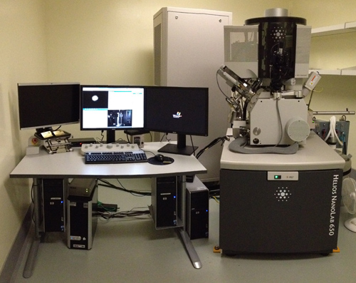
Helios NanoLab 650 FIB-SEM
The FEI Helios NanoLab 650 dual beam is a state of the art scanning electron microscope (SEM) and a focused ion beam (FIB) packaged in one, designed for extreme high resolution 2D and 3D characterisation, nanoprototyping and sample preparation.
Key features of the Helios NanoLab 650 dual beam at the CHTP
- Elstar XHR immersion lens FESEM column:
- Landing voltage range 50 V - 30 KeV
- Probe current 0.6 pA - 26 nA
- Resolution at optimum WD 1.5 nm at 200 V; 0.9 nm at 1 keV;
- 0.8 nm at 30 keV
- Beam deceleration with stage bias from -50 eV to -4 KeV
- Schottky thermal field emitter
- Tomahawk ion column with Gallium ion source with TOF correction and 2 stage differential pumping:
- Landing voltage range 500 V - 30 keV
- Probe current 1 pA - 65 nA (beam current density up to 60 A/cm²)
- Resolution 4.5 nm at 30 keV (preferred statistical method)
- Resolution 2.5 nm at 30 keV (selective edge method)
- Maximum horizontal field width:
- E-beam 2.3 mm
- I-beam 1.0 mm
- High precision 5 axes motorized stage:
- XY = 150 mm (repeatability (1.0 um)
- Z = 10 mm
- Tilt range -10 to +60 (accuracy 0.1° between 50-54°)
- Rotation 360°
- Chamber sample loading (approx 10 min):
- Sample size:
- 150 mm diameter with full rotation
- weight max. 500 g including sample holder
- Sample size:
- Quickloader loadlock (for fast sample transfer 3 min):
- Sample size:
- Max height 19 mm
- Max dia 33 mm
- FEI/Quorum CryoMAT quick loaded module providing rapid sample transfer and stage cryogenic cooling for heat sensitive samples.
- Sample size:
- IR chamber camera for real-time sample viewing
- Everhart-Thornley and Elstar in-lens secondary electron detector
- Retractable low voltage, high contrast solid state and Elstar-in-lens backscattered electron detector
- Retractable STEM detector with BF/DF/HAADF segments
- High performance secondary electron and secondary ion detector
- EDAX EBSD (Hikari XP camera and forward scattering detector) integrated system
- Pt deposition gas injection system
- Micromanipulators:
- Omniprobe 200 PC-controlled, closed loop multi-purpose nanopositioning system capable of in situ lift-out, electrical measurements, nanomechanical testing and charge neutralization in the FIB or SEM.
- NavCam correlative Navigation Unit
- Software:
- Auto slice and view software for automated sequential mill and view to collect series of images for 3D reconstruction.
- MAPS: a modular software application for automated acquisition of high resolution images from large areas, that converts your instrument into a high throughput image data production device.
- EDAX TEAM Pegasus analysis
- OIM Analysis ™
- Image Gallery
- SE
- BSE
- STEM
| Detector | Signal | Example |
| Everhart-Thornley | Secondary Electrons
(surface imaging) |
Slideshow 1 - True surface imaging conditions demonstrated with an anodized commercially pure titanium sample with the ET detector. Lowering the accelerating voltage stepwise from 1 keV, 500e V to 350 eV demonstrates the differences in the information obtained from the surface. |
| Backscattered Electrons (atomic number contrast) | Slideshow 2 - Surface imaging capability with backscattered electrons at 2 keV. | |
| Elstar in-lens | Secondary Electrons | Slideshow 3 - Comparative equivalents of high-resolution secondary (images 1 and 2) and backscattered (3 and 4) electron images demonstrated with anodized commercially pure titanium sample. |
| Backscattered Electrons | ||
| Retractable low voltage, high-contrast solid- state BSE detector | Backscattered Electrons (atomic number contrast) | Slideshow 4 - Low voltage backscattered imaging of commercially pure titanium. |
| STEM | Transmitted electrons Bright field/ Dark field / High Angle Annular Dark Field |
Slideshow 5 - STEM (in progress) |
| ICE | Secondary Electrons and Secondary Ions | Slideshow 6 - The ICE detector can image using secondary electrons and secondary ions. Oxides are usually visible with Secondary Ions. |
MORE INFORMATION
For more information about the capabilities and use of this machine, please send an e-mail.
BOOKING CALENDAR
Click here to view the booking calendar for the Helios 650 FIB-SEM...